High Voltage Automated Cable Tester Project
Key Specifications
Maximum Testing Voltage of 1kV
Automated Continuity and Insulation Testing
16 Channel
Leakage current testing
Modular Architecture
Introduction
This project is a fully self-designed and built high-voltage cable testing system developed to automate continuity and insulation verification for multi-core subsea and industrial cables. The system generates a controlled ~1 kV DC test voltage and performs precise, repeatable measurements across multiple channels, replacing slow and error-prone manual testing methods.
Designed from the ground up, the tester integrates modular hardware, isolated measurement architecture, and embedded control to ensure safe and reliable operation in demanding environments. The platform includes automated channel switching, precision current sensing, real-time diagnostics, and onboard logging, enabling clear pass/fail identification and traceable test data.
A key focus of the project was engineering robustness and scalability. The system uses a distributed microcontroller architecture, high-voltage-aware PCB design, and modular expansion capability, allowing it to scale to high channel counts while maintaining measurement integrity and electrical isolation.
This project demonstrates advanced skills in high-voltage electronics, mixed-signal measurement, embedded systems, and practical engineering design — from concept and schematic capture through to PCB layout, system integration, and real-world deployment.
Project Objectives
The primary goal of this project was to design a robust and scalable automated cable testing solution capable of operating safely at high voltage while maintaining measurement accuracy and repeatability.
Key objectives included:
Automating continuity and insulation resistance testing
Generating and controlling a stable ~1 kV DC test voltage
Ensuring electrical isolation and operator safety
Designing a modular architecture scalable to high channel counts
Providing clear pass/fail diagnostics and traceable results
Creating a field-deployable, engineering-grade system
Hardware Design
The hardware was designed with strong emphasis on high-voltage safety, measurement integrity, and modular expansion.
Key design elements:
High-voltage PCB layout with controlled creepage and clearance
Modular channel boards for scalability and maintainability
Precision current sensing and measurement circuitry
Protection and fault-handling hardware
Industrial enclosure and power architecture
Connectorized system for reliable field operation
The design balances electrical safety, measurement precision, and practical deployability.
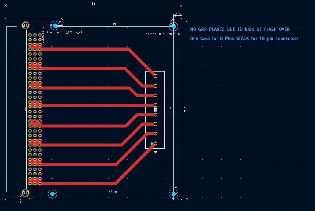
Connector Daughter Board
PCB Stackup
Main Board
Main PCB Stackup
The main control PCB was designed as a 6-layer controlled stackup to ensure signal integrity, high-voltage isolation, and measurement stability. The layer arrangement prioritises ground referencing, low-noise analog routing, and safe separation between high-voltage and logic domains.
Stackup Overview (Top → Bottom)
Layer 1 – Top Signal
Analog measurement routing
Critical signal traces
Guarded low-leakage paths
Controlled impedance where required
Layer 2 – Ground Plane (Solid)
Continuous reference plane
Low impedance return paths
Analog stability and noise suppression
Shielding for top layer signals
Layer 3 – Power Plane
24 V distribution
Regulated rails (12 V / 5 V / 3.3 V)
Segmented power domains
Controlled current return management
Layer 4 – Secondary Ground Plane
Dedicated analog/digital segmentation
Isolation boundary support
Reference plane for bottom routing
Layer 5 – Internal Signal / Control
Non-critical routing
Communication lines
Distributed control interconnect
Layer 6 – Bottom Signal
Low-speed routing
Interface connectors
System I/O